You’ve done everything by the book. Your stringing process is dialed in, your lamination parameters are perfect, and your handling procedures are flawless. Yet, when you run the final electroluminescence (EL) test, you see them: fine, dark lines snaking across the cells—microcracks.
It’s a frustratingly common scenario in solar module manufacturing. These defects can slash module efficiency and compromise long-term reliability. But what if the root cause isn’t in your process at all, but hidden in the geometry of the solar cells themselves, before they even reach your production line?
This is where cell warpage enters the picture—a subtle, often-invisible defect that sets off a powerful chain reaction of stress and failure.
The Invisible Culprit: Understanding Cell Warpage
At its core, cell warpage (or „bow“) is a deviation from perfect flatness. Think of a playing card with a slight, gentle curve. That’s essentially what happens to a solar cell. Thinner wafers, combined with the high-temperature processes used to create modern cells like PERC and TOPCon, introduce internal stresses that cause the silicon to deform.
While a slight bow might seem harmless, it’s a ticking time bomb. As a warped cell enters the automated stringing and layup process, machinery forces it flat. This flattening action induces significant mechanical stress across the cell’s surface, priming it for fracture.
The real problem? You can’t reliably see it with the naked eye. To truly understand the risk, you need to measure it.
Seeing the Unseen: Quantifying Warpage with 3D Laser Scanning
This is where advanced diagnostics come into play. High-precision 3D laser scanners can create a detailed topographical map of a solar cell’s surface. This isn’t just a picture; it’s a data-rich model that measures height variations down to the micron level.
This 3D map instantly reveals the extent and location of any warpage. It clearly shows areas of high elevation (the peak of the bow) and low elevation (the edges), pinpointing exactly where stress will concentrate during assembly.
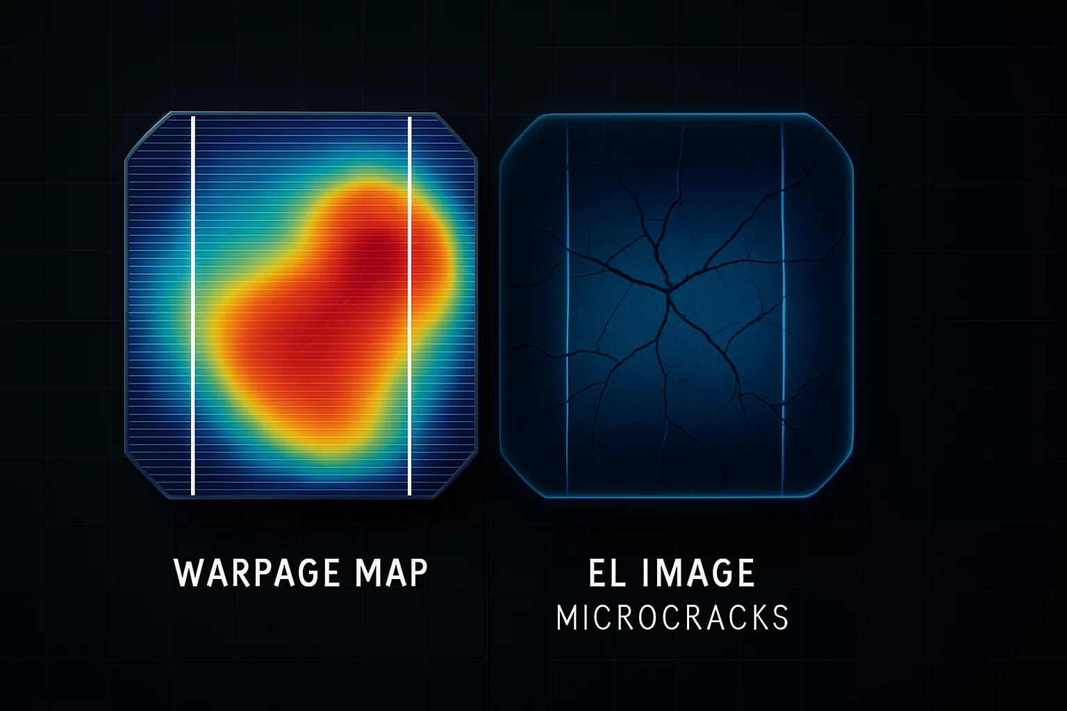
In the scan above, the red and yellow areas represent the highest points of the bow, while the blue areas are the lowest. This simple visualization transforms an invisible problem into a measurable and predictable risk factor.
The Moment of Truth: From Stress to Cracks
A solar module is a sandwich of materials: glass, encapsulant, cells, another layer of encapsulant, and a backsheet. During lamination, this stack is heated and pressed together under vacuum to create a solid, weatherproof unit.
For a warped cell, this is the moment of reckoning.
As the laminator presses the stack together, it forcefully flattens the curved cell against the rigid glass. The internal stresses introduced by this action are now „locked in.“ Since silicon is a brittle crystalline material, it can’t absorb this strain. Instead, it cracks.
This is the critical link: the pre-existing geometric flaw (warpage) transforms into damaging mechanical stress during assembly, leading directly to microcracks.
Connecting the Dots: Correlating 3D Scans with EL Images
The final piece of the puzzle comes from electroluminescence (EL) testing. By passing a current through the finished module, we can make the cells light up, much like an LED. Healthy, undamaged areas shine brightly, while cracks, breaks, and other defects appear as dark or inactive areas.
When we place a cell’s initial 3D scan next to its final EL image after lamination, the connection becomes undeniable.
The pattern is unmistakable: the microcracks in the EL image consistently appear along the areas of highest stress predicted by the 3D warpage map. These cracks often form parallel to the busbars, where the cell experiences the most significant bending force.
This direct correlation proves that a cell’s initial geometry is a primary driver of microcracks—a fundamental insight for robust solar module prototyping and effective incoming quality control for new cell batches.
Why This Matters for Your Production Line
Understanding this cause-and-effect relationship moves cell quality control from a reactive to a predictive strategy. Instead of just finding cracks at the end of the line, you can prevent them from ever forming.
- Smarter Incoming Quality Control (IQC): Don’t rely solely on supplier datasheets. Implementing 3D geometric checks for incoming cells allows you to quantify warpage and set acceptance thresholds, screening out high-risk batches before they cost you time and money.
- Reduced Yield Loss: Every cracked cell in a module is a potential point of failure, leading to rejection or power loss. Catching warped cells early protects your production yield and reduces waste.
- Enhanced Long-Term Reliability: Microcracks that are small at the time of manufacturing can grow over years of thermal cycling and mechanical stress in the field, leading to power degradation and premature module failure. Building with flatter, lower-stress cells results in a more durable and reliable final product.
Frequently Asked Questions (FAQ)
What causes solar cell warpage in the first place?
Warpage is primarily caused by thermal stresses introduced during the high-temperature steps of cell manufacturing, such as diffusion, annealing, and firing of metal pastes. As cells become thinner to save on silicon costs, they become more susceptible to this type of deformation.
Is all cell warpage bad? Is there an acceptable tolerance?
Not all warpage leads to cracking. There is typically an acceptable tolerance, but it depends on the cell thickness, cell technology, and the specific stringing and lamination processes used. A key goal of process validation is to determine a maximum allowable warpage for your specific production line.
Can’t you just see warpage by eye?
No. Significant warpage might be visible if you hold a cell at an angle to a light source, but minor, high-risk warpage is often impossible to detect visually. Only precise measurement tools like 3D laser scanners can provide the quantitative data needed for effective quality control.
What’s the difference between a microcrack and a full break?
A microcrack is a very fine fracture in the silicon wafer that may not be visible to the naked eye. It creates an electrically inactive area but may not separate the cell into pieces. A full break, or fracture, physically separates a piece of the cell, leading to a complete disruption of the electrical path. Both are detected by EL testing.
How does this affect different cell technologies like PERC, TOPCon, or HJT?
While warpage can affect any cell technology, advanced architectures like TOPCon and HJT involve additional processing layers and thermal steps that can influence internal stress. Furthermore, as all these technologies move toward ultra-thin wafers, the sensitivity to warpage-induced stress generally increases.
The Path to Smarter Quality Control
The mystery of unexplained microcracks is often solved by looking beyond the assembly line and focusing on the intrinsic properties of the materials themselves. By understanding and measuring initial cell warpage, manufacturers can take a crucial step toward building more efficient, reliable, and profitable solar modules.
This is a perfect example of how applied research—connecting precise laboratory measurements with real-world production conditions—can uncover the insights needed to solve the industry’s most persistent challenges and accelerate innovation.